PCB design with KiCad
KiCad is an open-source Electronic Design Automation (EDA) suite used for designing schematics and PCBs.
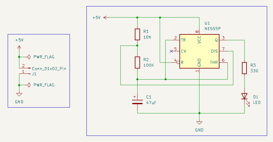
In this post, I will use a breathing LED circuit using NE555 as an example to show how to use the KiCad.
Project Setup
The first thing to do is to create a new project.
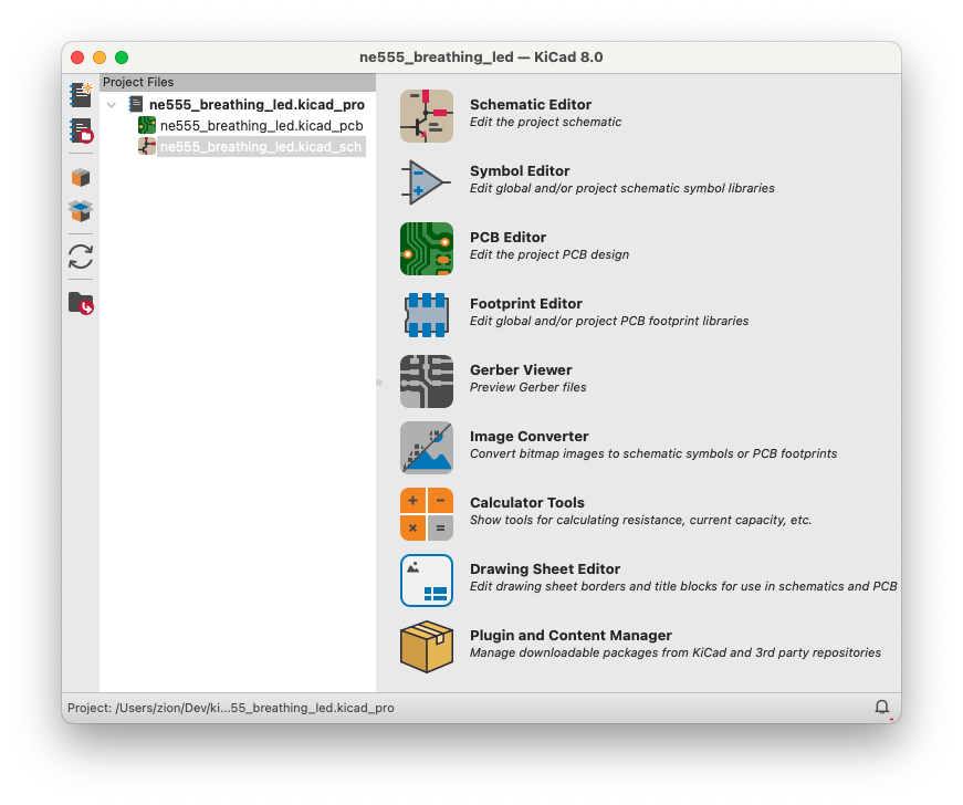
After creating the project, the “Project Files” pane on the left will show a project file with the extension .kicad_pro, a schematic file with the extension .kicad_sch and a schematic file with the extension .kicad_pcb.
Schematic Design
-
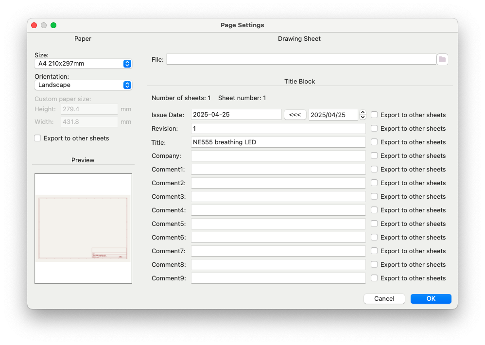
Setup the page
- Add symbols by clicking the
 button or use the hotkey
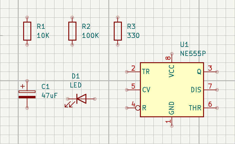
 A. Symbols are automatically annotated when added to the schematic. - Arrange symbols by moving and rotating them. Then fill in the values of the component as needed.
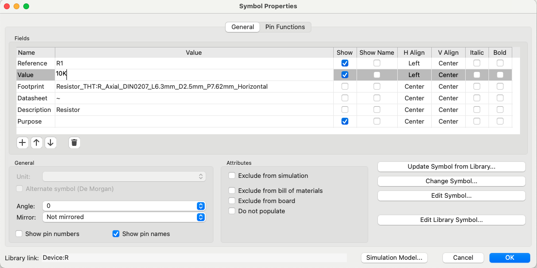
You can change the value of the component by double-clicking the component to open the Symbol Properties window.
- Assign footprints to symbols using the footprint assignment tool. Clicking
Tools → Assign Footprints…or using the button in the top toolbar.
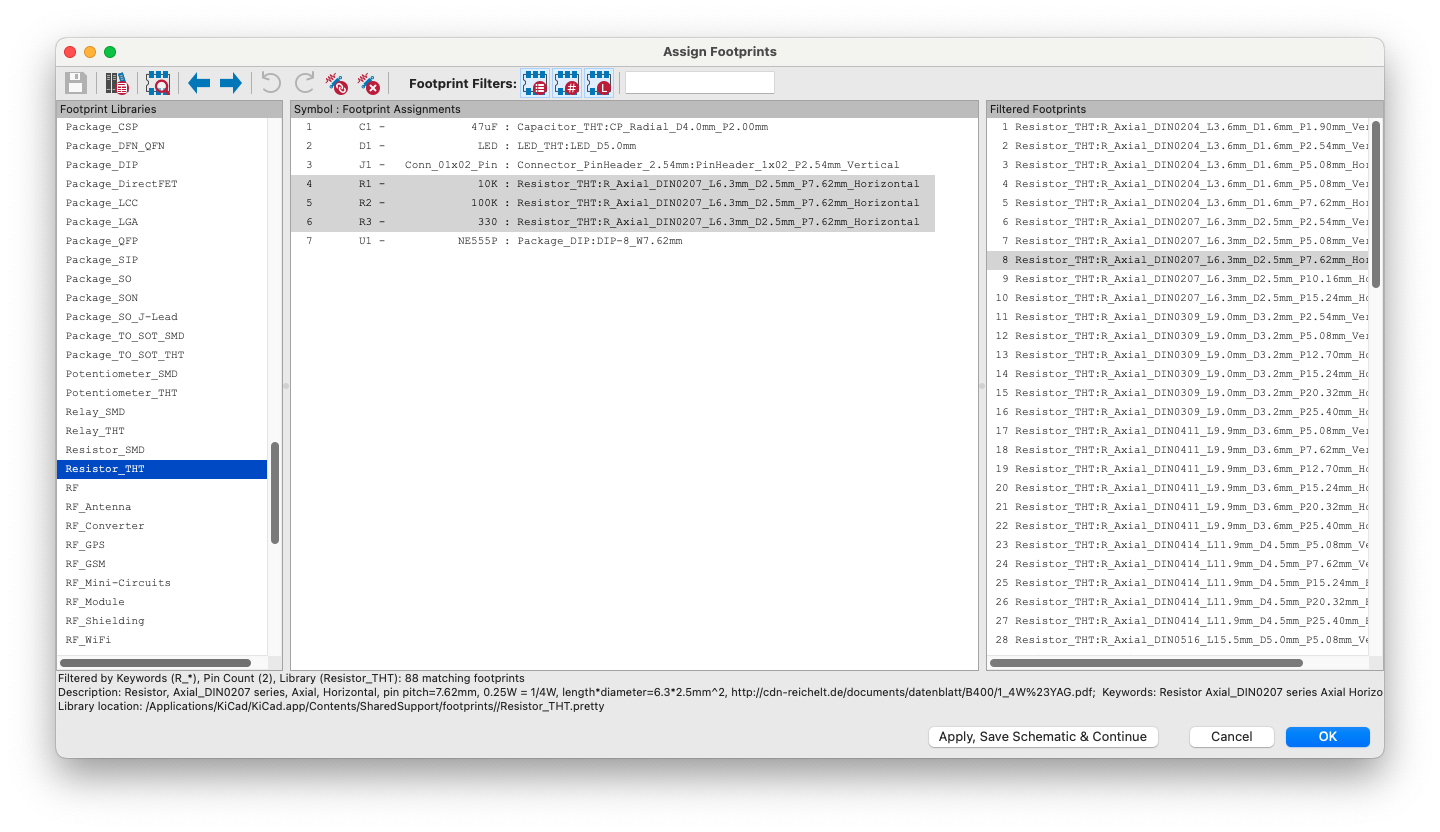
Select the symbol in the middle pane and double-click the desired footprint in the right pane. You can also preview the footprint by right-clicking the footprint’s name and selecting View selected footprint.
-
Connect components with wires.
-
Run an electrical rule check (ERC) to verify the design.
PCB Layout Design
- Setup the page
- Click
Tools → Update PCB from Schematic…or using the button in the top toolbar to import the schematic design data into the layout.
 - Place the components and draw a board outline on the
Edge.Cutslayer. - Route the connections (tracks) by clicking the
 button in the right toolbar or use the hotkey
 X. - Place the copper zones. Switch to the
B.Culayer and click the button in the right toolbar.
When you click on the PCB, the Copper Zone Properties dialog will appear, select the GND net.
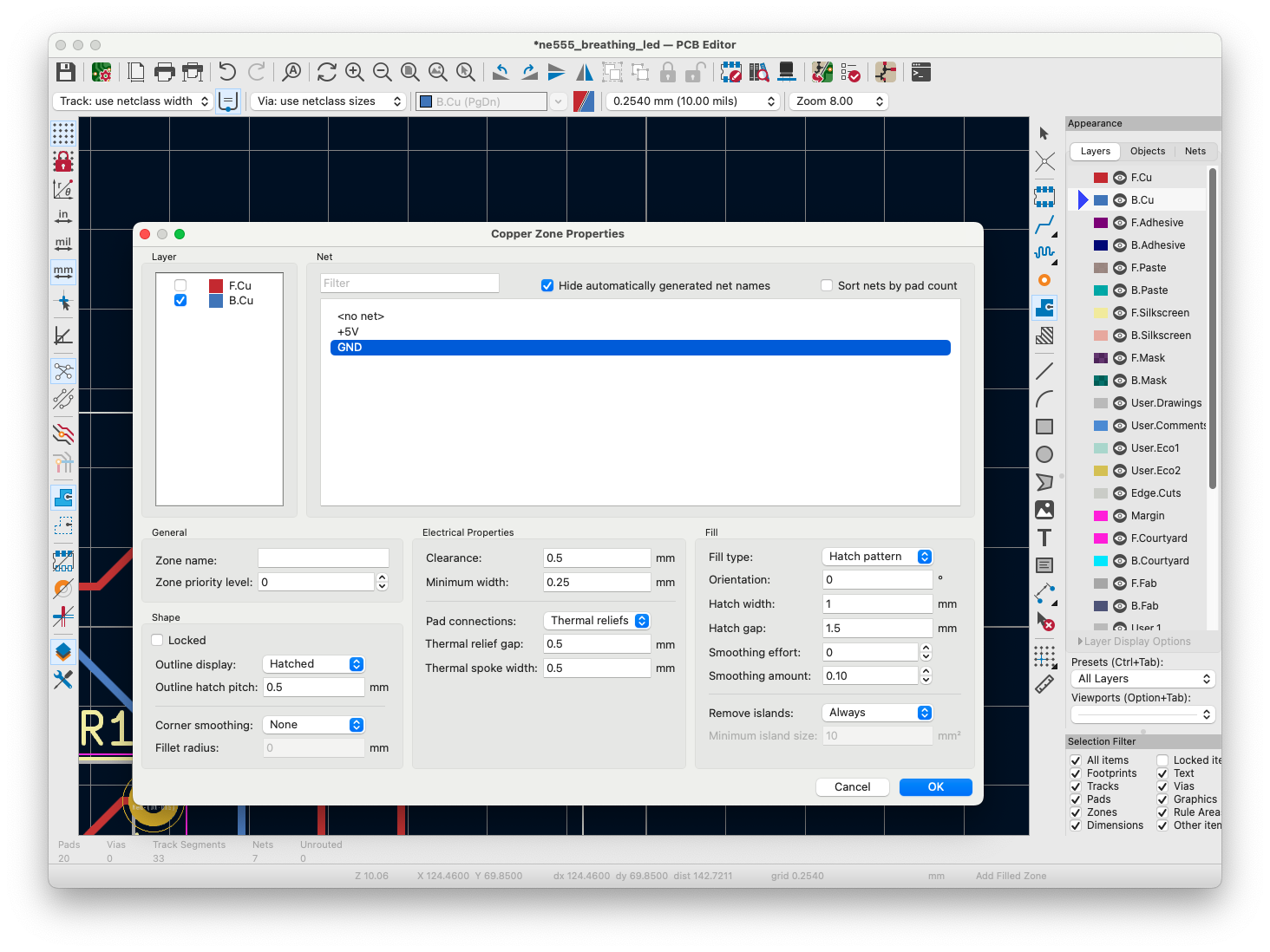
Draw an outline that defines the boundaries of the zone, then right click it and select Zones → Draft Fill Selected Zone(s).
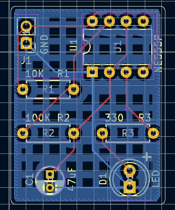
Zones can be hidden by click the  button in the left toolbar.
- Add silkscreen text, logos, or other markings.
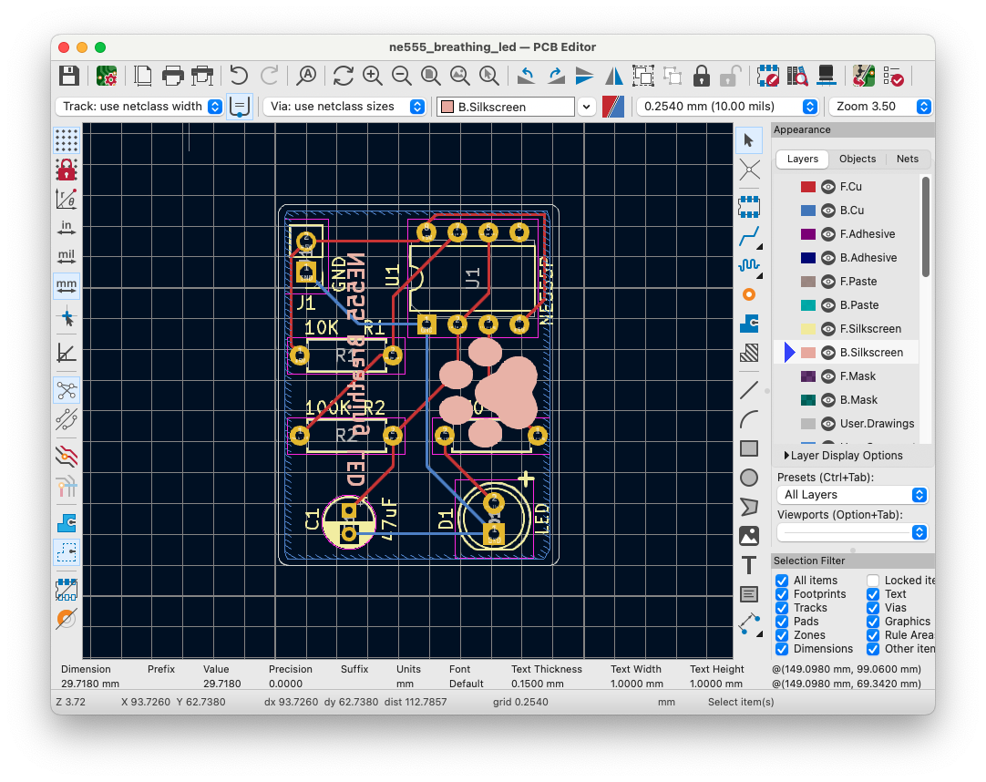
- Run a Design Rules Check (DRC) to verify the correctness of the layout.
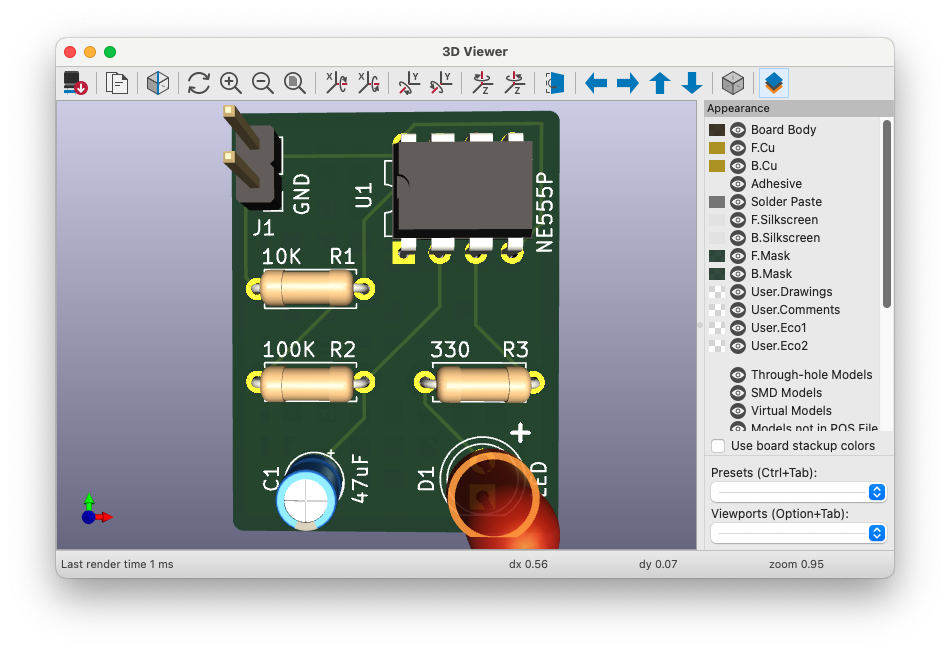
- Use the 3D viewer (
View → 3D Viewer) to visualize the design.
Generate Fabrication Outputs
Click File → Plot… or File → Fabrication Outputs → Gerbers (.gbr)… to open the Plot dialog.
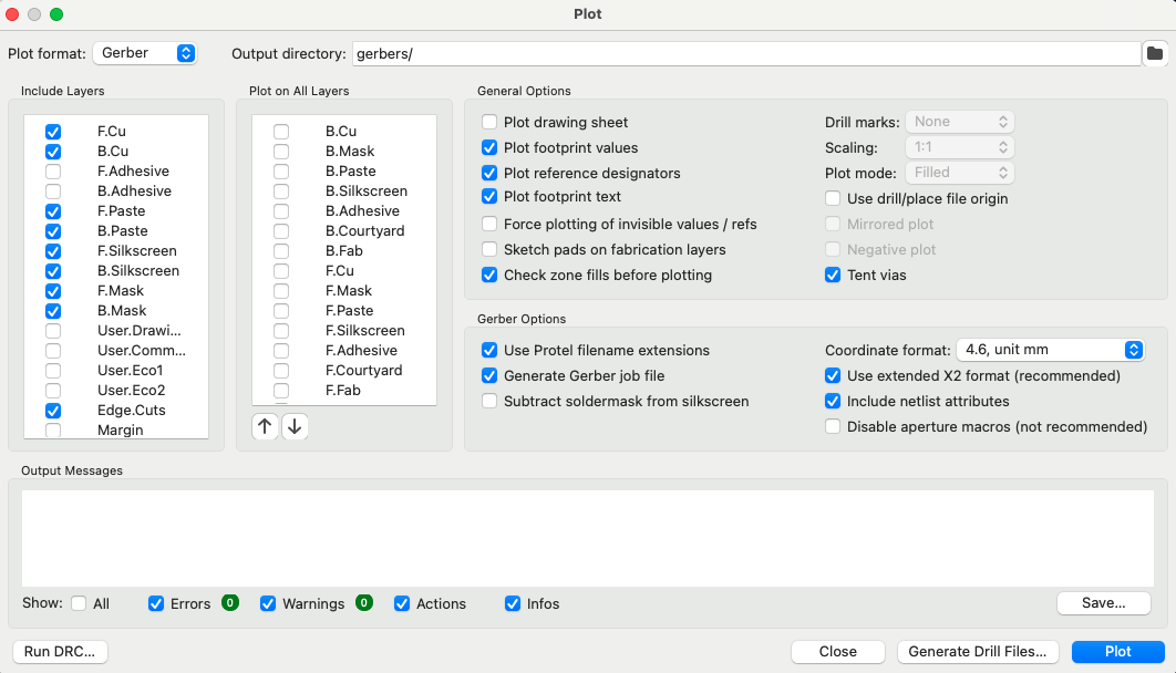
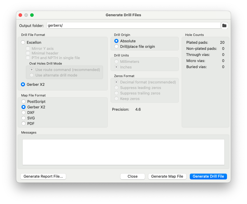
Click Plot to generate the Gerber files. Also click Generate Drill Files… to create drill files for through-holes and vias.
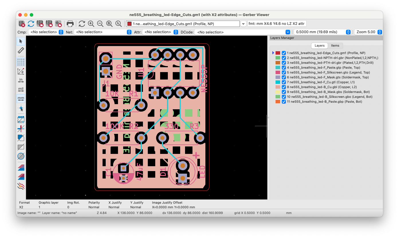
You can check the generated Gerber files with Gerber Viewer.